UCC27211A
UCC27211A is 3.7A/4.5A Half-Bridge Driver manufactured by Texas Instruments.
SLUSBL4D
- AUGUST 2013
- REVISED JULY 2024
UCC27211A 120V, 3.7A/4.5A Half-Bridge Driver with 8V UVLO
CONTROL
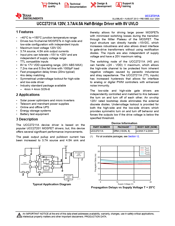
Propagation Delay (ns)
1 Features
- - 40°C to +150°C junction temperature range
- Drives two N-channel MOSFETs in high-side and low-side configuration with independent inputs
- Maximum boot voltage 120V DC
- 3.7A source, 4.5A sink output currents
- Input pins can tolerate
- 10V to +20V and are independent of supply voltage range
- TTL patible inputs
- 8V to 17V VDD operating range, (20V ABS MAX)
- 7.2ns rise and 5.5ns fall time with 1000pF load
- Fast propagation delay times (20ns typical)
- 4ns delay matching
- Symmetrical undervoltage lockout for high-side and...